In a nutshell, Kioxia proposes to avoid dicing, assembly, chip packaging, and SSD drive assembly, however use a whole wafer with 3D NAND instead..
The wafer is to be penetrated utilizing Kioxias very multi-probing technology to find in addition to disable faulty 3D NAND dies and then connected to a pad with I/O and power connectors. The whole thing ought to be operated in parallel to extract optimum consecutive and random IOPS efficiency.
The existing capability of SSDs is restricted by form-factors and chip product packaging technologies, whereas efficiency boundaries are specified by controllers (i.e., by the number of their NAND channels in addition to their capability to efficiently perform ECC and other necessary operations quickly) and the PCI Express interface..
On a wafer level, one can get a severe variety of NAND channels (believe well beyond Microsemis 32 channels common on enterprise-grade SSDs), whereas a PCIe 6.0 x16 user interface would deliver up to 128 GB/s of bandwidth. When it comes to IOPS, we are talking about a multi-channel monstrous SSDs, so think about millions of IOPS.
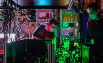
( Image credit: Blocks & & Files) Shigeo Oshima, Kioxias primary engineer, described the concept of wafer-level SSDs in a presentation at VLSI Symposium 2020, suggesting this is not a product from the companys roadmap, but ideally something to come quickly.
Kioxia currently produces 1.33 Tb 96-layer 3D QLC NAND chips that measure 158.4 mm2 and deliver up to a 132 MB/s write efficiency due to a quad-plane architecture. Roughly 355 of such passes away fit on a 300-mm wafer, so assuming a yield rate of approximately 90%, Toshiba navigates 320 good dies, or 53 TB of raw 3D QLC NAND. With future models, Toshiba will have even more raw 3D NAND per wafer.
A solid-state storage service based upon 300-mm 3D NAND wafer( s) would look like a standard rack server with its own reasoning, PSU, cooling system, and other components like network user interfaces. From storage density perspective, such a server is not going to be a champion (not in a world where you can load 100 TB into a 3.5-inch form-factor), however if you require severe performance at a relatively low cost, a gadget of such kind could make sense.
Likewise have a look at our total list of the finest company laptops: top devices for working from house, SMB and more.
Via Blocks & & Files.
Kioxia presently produces 1.33 Tb 96-layer 3D QLC NAND chips that determine 158.4 mm2 and provide up to a 132 MB/s write performance due to a quad-plane architecture. Approximately 355 of such dies fit on a 300-mm wafer, so assuming a yield rate of approximately 90%, Toshiba gets around 320 excellent dies, or 53 TB of raw 3D QLC NAND. With future iterations, Toshiba will have even more raw 3D NAND per wafer.
Modern hyperscale datacenters have infinite cravings for storage capacity, density, and performance, which is why numerous new SSD form-factors created to take full advantage of performance and capacity were presented in the current years..
Kioxia thinks that there is a quicker and less expensive method to provide preferred solid-state storage services to cloud consumers: wafer-level SSDs..
With capabilities beginning at around 50 TBs utilizing current 3D QLC NAND, such gadgets might provide unbeatable performance.
Wafer-level SSDs.