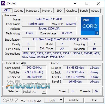
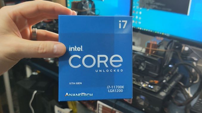
The march on performance with desktop platforms has unique challenges compared to other platforms. Peak single thread throughput is often considered the Holy Grail, with a fast follow up of good multi-core and all-core performance given the nature of how desktop platforms are used with background processes and multiple concurrent applications. In order to bring its best single core performance to the desktop market, Intel had to redesign its 10nm product on 14nm, which combines the high throughput of the design with the high frequency of 14nm. These redesigned Cypress Cove cores form the basis of Intel’s new 11th Gen Desktop Processor Family, Rocket Lake. Today we are reviewing the Core i7-11700K, an eight-core processor with hyperthreading able to boost up to 5.0 GHz.
Notice
The official launch date for these processors, and full reviews, is March 30th. We are currently under NDA with Intel for the information that has been provided by Intel, and will publish that information in due course. However, as noted in a number of press outlets, some units have already been sold at retail before that sales date. Units obtained by that method are not under NDA by definition, and we obtained the Core i7-11700K for this review at retail, and as such we are not under NDA for any information we have obtained through using this processor.
Before publishing this review, we gave Intel advance notice to respond to us having a full review ahead of the formal release. Our email seemingly generated some excitement inside (and to our surprise, outside) Intel, but we received a response from Intel stating that they had no comment to offer.
Rocket Lake We Know About
Core i9-11900K and Core i7-11700K
Back at the start of the year, during CES, Intel disclosed product information about its lead halo product on the Rocket Lake platform, the Core i9-11900K. This includes some microarchitecture details, as well as core count, frequency, memory, graphics, and features relating to IO and the chipset. With our review here today, we can add the 11700K to that data with what we can probe from the processor.
| AnandTech | Core i9-11900K | Core i7-11700K |
| SoC | Rocket Lake | Rocket Lake |
| Microarchitecture | Cypress Cove | Cypress Cove |
| Cores / Threads | 8 / 16 | 8 / 16 |
| TDP | 125 W | 125 W |
| Base Frequency | ? | 3600 MHz |
| Turbo 2.0 (1-2 C) | ? | 4900 MHz |
| Turbo 3.0 (1-2 C) | ? | 5000 MHz |
| Thermal Velocity Boost | 5300 MHz | – |
| All Core Turbo | 4800 MHz | 4600 MHz |
| DDR4 | 2 x DDR4-3200 | 2 x DDR4-3200 |
| GPU + EUs | Xe-LP, 32 EUs | Xe-LP, 32 EUs |
| PCIe | 4.0 x16 + 4.0 x4 | 4.0×16 + 4.0 x4 |
| AVX-512 | Yes | Yes |
| Price | ? | We paid equivalent $469 |
The differences between the two Rocket Lake processors, based on available information, are slim. The main difference is that the Core i9 is known to have Intel’s Thermal Velocity Boost technology, however the Core i7 does not – this means the peak frequency is only 5.0 GHz, not 5.3 GHz. The all core frequency is only 200 MHz different.
The new generation Rocket Lake is the combination of two different backported technologies. Intel took the Sunny Cove core from 10nm Ice Lake, and re-built it on 14nm, calling it now Cypress Cove. Intel also took the Xe graphics from 10nm Tiger Lake and re-built those on 14nm, but these are still called Xe graphics.
We can see that the new design is an amalgam of new technologies, by comparing Rocket Lake to Comet Lake, Ice Lake, and Tiger Lake:
| Microarchitecture Comparison | |||||
| AnandTech | Comet Lake | Rocket Lake | Ice Lake | Tiger Lake | Ryzen 5000 |
| Form Factor | Desktop | Desktop | Laptop | Laptop | Desktop |
| Max Cores | 10 | 8 | 4 | 4 | 16 |
| TDP | 125 W | 125 W | 28 W | 35 W | 105 W |
| uArch | Comet | Cypress | Sunny | Willow | Zen 3 |
| IGP | Gen 9 | Xe-LP | Gen 11 | Xe | – |
| IGP Cores | 24 | 32 | 64 | 96 | – |
| L1-D | 32 KB /c | 48 KB /c | 48 KB /c | 48 KB/c | 32 KB/c |
| L2 Cache | 256 KB /c | 512 KB /c | 512 KB/c | 1280KB /c | 512 KB/c |
| L3 Cache | 20 MB | 16 MB | 8 MB | 12 MB | 64 MB |
| PCIe | 3.0 x16 | 4.0 x20 | 3.0 x8 | 4.0 x4 | 4.0 x24 |
| DDR4 | 2 x 2933 | 2 x 3200 | 2 x 3200 | 2 x 3200 | 2 x 3200 |
| LPDDR4X | – | – | 4 x 3733 | 4 x 4266 | – |
There are obviously some differences between the notebook and desktop parts, most noticeably that the new platform at the high-end has only eight cores, two fewer than Comet Lake.
This is because Intel found 8 cores to be the best balance of die area, power consumption, performance, and cost. Several times I’ve seen Intel spokespeople say the reason for 8 cores being ‘the most we could fit’, although that’s categorically false. More cores can be added, but overall they would run at a lower frequency for the same power, the interconnect might not scale, or the die size/yield would raise the price too much. The phrase ‘the most we could fit’, by all technical understanding, is a steaming pile. It needs additional qualifiers, or to simply say ‘the best fit given die area, yield, and cost’.
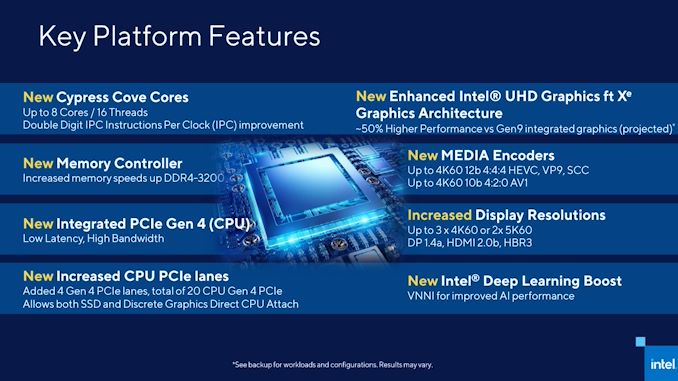
Additional improvements over Comet Lake include AVX512 units, support for 20 PCIe 4.0 lanes, and faster memory. With the new chipsets, Intel has already disclosed that the Rocket Lake platform will have native USB 3.2 Gen 2×2 (20 Gbps), and with the Z590 motherboards, a double bandwidth link from CPU to the chipset, moving from DMI x4 to DMI x8, effectively a PCIe 3.0 x8 link.
Rocket Lake on 14nm: The Best of a Bad Situation
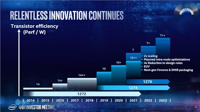
The delays around the viability of Intel’s 10nm manufacturing have been well documented. To date, the company has launched several products on its 10nm process for notebooks, such as Cannon Lake, Ice Lake, Jasper Lake, Elkhart Lake, and Tiger Lake. There have been other non-consumer products, such as Agilex FPGAs and Snow Ridge 5G SoCs, and Intel has confirmed that its 10nm server products ‘Ice Lake Xeon Scalable’, are currently in volume production for a late Q1 launch.
The one product line missing from that list is the desktop and enthusiast segments that typically use socketed processors paired with discrete graphics. Intel has always committed to launching desktop processors on its 10nm process, however we are yet to see the results of their efforts. The issues Intel is having with 10nm have never been fully elaborated on, with Intel instead opting to promote some of the improvements made, such as its new SuperFin technology, which is in Tiger Lake and the next-generation server platform beyond Ice Lake Xeon Scalable (for those keeping track, that would be Sapphire Rapids). The 10nm improvements so far has enabled Intel to launch notebook processors and server processors, both of which have lower power-per-core than a typical desktop offering.
As 10nm has not been able to meet the standards required for desktop-level performance, rather than leave a potential 3 year gap in the desktop product family, Intel has been in a holding pattern releasing slightly upgraded versions of Skylake on slightly improved variants of 14nm. The first two members of the Skylake family, Skylake and Kaby Lake were released as expected. While waiting, we saw Intel release Coffee Lake, Coffee Lake Refresh, and Comet Lake. Each of these afforded minor updates in frequency, or core count, or power, but very little in the way of fundamental microarchitectural improvement. The goal all along was to move to 10nm with the same architecture as the mobile Ice Lake processors, but that wasn’t feasible due to manufacturing limitations limiting how well the processors scaled to desktop level power.
With previous generations, Intel traditionally had either upgraded the process node technology, or updated the microarchitecture – a process that Intel called Tick-Tock. Originally Intel was set to perform a normal ‘Tick’ after Kaby Lake, and have Cannon Lake with the same effective Skylake microarchitecture move to 10nm. Cannon Lake ending up only as a laptop processor with no working graphics in a small number of notebooks in China as it was a hot mess (as shown in our review). As a result, Intel refocused its 10nm for notebook processors hoping that advances would also be applicable to desktop, but the company had to release minor upgrades on desktop from Coffee Lake onwards to keep the product line going.
This meant that at some level Intel knew that it would have to combine both a new architecture and a new process node jump into one product cycle. At some point however, Intel realized that the intercept point with having a new microarchitecture and the jump for the desktop to 10nm was very blurry, and somewhat intangible, and at a time when its main competitor was starting to make noise about a new product that could reach parity in single core performance. In order to keep these important product lines going, drastic measures would have to be taken.
After many meetings with many biscuits, we presume, the decision was made that Intel would take the core microarchitecture design from 10nm Ice Lake, which couldn’t reach high enough frequencies under desktop power, and repackage that design for the more dependable 14nm node which could reach the required absolute performance numbers. This is known as a ‘backport’.
Sunny Cove becomes Cypress Cove
The new Core 11th Gen processor which we are looking at today has the codename Rocket Lake. That’s the name for the whole processor, which consists of cores, graphics, interconnect, and other different accelerators and IP blocks, each of which also have their own codenames, just for the sake of making it easier for the engineers to understand what parts are in use. We use these codenames a lot, and the one to focus on here is the CPU core.
Intel’s 10nm Ice Lake notebook processor family uses Sunny Cove cores in the design. It is these cores that have been backported to 14nm for use in the Rocket Lake processors, and because it is on a different process node and there are some minor design changes, Intel calls them Cypress Cove cores.
The reason behind this is because taking a design for one manufacturing process and designing it for a second is no easy task, especially if it’s a regressive step – transistors are bigger, which means logic blocks are bigger, and all the work done with respect to signaling and data paths in the silicon has to be redone. Even with a rework, signal integrity needs to be upgraded for longer distances, or additional path delays and buffers need to be implemented. Any which way you cut it, a 10nm core is bigger when designed for 14nm, consumes more power, and has the potential to be fundamentally slower at execution level.
Intel’s official disclosures to date on the new Cypress Cove cores and Rocket Lake stem from a general briefing back in October, as well as a more product oriented announcement at CES in January. Intel is promoting that the new Cypress Cove core offers ‘up to a +19%’ instruction per clock (IPC) generational improvement over the cores used in Comet Lake, which are higher frequency variants of Skylake from 2015. However, the underlying microarchitecture is promoted as being identical to Ice Lake for mobile processors, such as caches and execution, and overall the new Rocket Lake SoC has a number of other generational improvements new to Intel’s desktop processors.
In This Review, and Limitations
As mentioned at the outset, this is a review prior to the official review embargo for these processors. We are able to post this outside of the NDA as we were able to obtain the hardware at retail. There is still a lot of information that has not been disclosed, the sort of thing that normally accompanies a new processor launch, and whatever Intel has told is still part under NDA – details of which are also under the same NDA. So we won’t be able to go into those just yet, but we can start to fire some benchmark data at you. In this review we’re focusing mainly on the generational 8-core offerings across a number of products and generations.
| 8-Core CPU Comparison | ||||||
| AnandTech | Core i9-9900KS | Core i7-10700K | Core i7-11700K | Ryzen 7 5800X | Ryzen 7 4750G | |
| uArch | Coffee Refresh | Comet Lake | Cypress Cove | Zen 3 | Zen 2 + Vega | |
| Cores | 8 C / 16 T | 8 C / 16 T | 8 C / 16 T | 8 C / 16 T | 8 C / 16 T | |
| Base Freq | 4000 | 3800 | 3600 | 3800 | 3600 | |
| Turbo Freq | 5000 | 5100 | 5000 | 4800 | 4400 | |
| All-Core | 5000 | 4700 | 4600 | ~4550 | ~4150 | |
| TDP | 127 W | 125 W | 125 W | 105 W | 65 W | |
| IGP / EUs | Gen 9, 24 | Gen 9, 24 | Xe-LP, 32 | – | Vega, 8 | |
| L3 Cache | 16 MB | 16 MB | 16 MB | 32 MB | 8 MB | |
| DDR4 | 2 x 2666 | 2 x 2933 | 2 x 3200 | 2 x 3200 | 2 x 3200 | |
| PCIe | 3.0 x16 | 3.0 x16 | 4.0 x20 | 4.0 x24 | 3.0 x8 | |
| MSRP | $513 box | $387 box | ? | $449 SEP | ~$345 | |
We paid 394€ for our processor pre-tax, which comes to $469. We suspect this is well above Intel’s recommended retail price, given that this was sold before the official sales date and demand for high performance processors is very high.
Test Setup and #CPUOverload Benchmarks
As per our processor testing policy, we take a premium category motherboard suitable for the socket, and equip the system with a suitable amount of memory running at the manufacturer’s maximum supported frequency. This is also run at JEDEC subtimings where possible. Reasons are explained here.
| Test Setup | |||||
| Intel Rocket Lake | Core i7-11700K | – | – | TRUE Copper + SST* | ADATA 4×32 GB DDR4-3200 |
| Intel Comet Lake | Core i7-10700K | – | – | TRUE Copper + SST* | ADATA 4×32 GB DDR4-2933 |
| Intel Coffee Refresh | Core i9-9900KS | MSI MPG Z390 Gaming Edge AC | AB0 | TRUE Copper +SST* | ADATA 4x32GB DDR4-2666 |
| AMD AM4 | Ryzen 7 5800X Ryzen 7 4750G | GIGABYTE X570I Aorus Pro | F31L | Noctua NHU-12S SE-AM4 | ADATA 4×32 GB DDR4-3200 |
| GPU | Sapphire RX 460 2GB (CPU Tests) NVIDIA RTX 2080 Ti FE (Gaming Tests) | ||||
| PSU | Corsair AX860i | ||||
| SSD | Crucial MX500 2TB | ||||
| *TRUE Copper used with Silverstone SST-FHP141-VF 173 CFM fans. Nice and loud. **Other CPUs in graphs tested in same systems for CPU family | |||||
While we can’t disclose the motherboard used due to NDA reasons, it has already been announced by the manufacturer. Meanwhile, the BIOS used is likely not the final variant that will be used for Rocket Lake’s retail launch later this month, and further BIOSes may contain potential minor adjustments to performance or turbo responses.
We must thank the following companies for kindly providing hardware for our multiple test beds. Some of this hardware is not in this test bed specifically, but is used in other testing.
A big thanks to ADATA for the AD4U3200716G22-SGN modules for this review. They’re currently the backbone of our AMD testing.
Users interested in the details of our current CPU benchmark suite can refer to our #CPUOverload article which covers the topics of benchmark automation as well as what our suite runs and why. We also benchmark much more data than is shown in a typical review, all of which you can see in our benchmark database. We call it ‘Bench’, and there’s also a link on the top of the website in case you need it for processor comparison in the future.
Table Of Contents
Note: If you’ve reached this far, great! This is not the end of the review. We have over a dozen pages with data and benchmark results, as well as a conclusion. They are all in the drop down box below.

