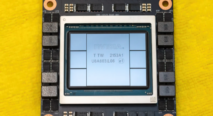
At GTC 2022, NVIDIA unveiled its Hopper H100 GPU, a compute powerhouse designed for the next generation of data centers. It’s been a while since we talked about this mighty chip but it looks like NVIDIA gave a close-up of its flagship chip to select media.
NVIDIA Hopper H100 GPU: First With 4nm and HBM3 Technology Gets High-Res Pictures
CNET managed to get hold of not only the graphics board on which the H100 GPU is fused but also the H100 chip itself. The H100 GPU is a monster chip that comes packed with the latest 4nm tech and incorporates 80 Billion transistors along with the bleeding-edge HBM3 memory technology. As per the tech outlet, the H100 is built upon the PG520 PCB board which has over 30 power VRMs & a massive integral interposer that uses TSMC’s CoWoS tech to combine the Hopper H100 GPU with a 6-stack HBM3 design.
NVIDIA Hopper H100 GPU Pictured (Image Credits: CNET):
Out of the six stacks, two stacks are kept to ensure yield integrity. But the new HBM3 standard allows for up to 80 GB capacities at 3 TB/s speeds which are crazy. For comparison, the current fastest gaming graphics card, the RTX 3090 Ti, offers just 1 TB/s of bandwidth and 24 GB VRAM capacities. Other than that, the H100 Hopper GPU also packs in the latest FP8 data format, and through its new SXM connection, it helps accommodate the 700W power design that the chip is designed around.
NVIDIA Hopper H100 GPU Specifications At A Glance
So coming to the specifications, the NVIDIA Hopper GH100 GPU is composed of a massive 144 SM (Streaming Multiprocessor) chip layout which is featured in a total of 8 GPCs. These GPCs rock total of 9 TPCs which are further composed of 2 SM units each. This gives us 18 SMs per GPC and 144 on the complete 8 GPC configuration. Each SM is composed of up to 128 FP32 units which should give us a total of 18,432 CUDA cores. Following are some of the configurations you can expect from the H100 chip:
The full implementation of the GH100 GPU includes the following units:
- 8 GPCs, 72 TPCs (9 TPCs/GPC), 2 SMs/TPC, 144 SMs per full GPU
- 128 FP32 CUDA Cores per SM, 18432 FP32 CUDA Cores per full GPU
- 4 Fourth-Generation Tensor Cores per SM, 576 per full GPU
- 6 HBM3 or HBM2e stacks, 12 512-bit Memory Controllers
- 60 MB L2 Cache
- Fourth-Generation NVLink and PCIe Gen 5
The NVIDIA H100 GPU with SXM5 board form-factor includes the following units:
- 8 GPCs, 66 TPCs, 2 SMs/TPC, 132 SMs per GPU
- 128 FP32 CUDA Cores per SM, 16896 FP32 CUDA Cores per GPU
- 4 Fourth-generation Tensor Cores per SM, 528 per GPU
- 80 GB HBM3, 5 HBM3 stacks, 10 512-bit Memory Controllers
- 50 MB L2 Cache
- Fourth-Generation NVLink and PCIe Gen 5
This is a 2.25x increase over the full GA100 GPU configuration. NVIDIA is also leveraging from more FP64, FP16 & Tensor cores within its Hopper GPU which would drive up performance immensely. And that’s going to be a necessity to rival Intel’s Ponte Vecchio which is also expected to feature 1:1 FP64.
The cache is another space where NVIDIA has given much attention, upping it to 48 MB in the Hopper GH100 GPU. This is a 20% increase over the 50 MB cache featured on the Ampere GA100 GPU and 3x the size of AMD’s flagship Aldebaran MCM GPU, the MI250X.
Rounding up the performance figures, NVIDIA’s GH100 Hopper GPU will offer 4000 TFLOPs of FP8, 2000 TFLOPs of FP16, 1000 TFLOPs of TF32 and 60 TFLOPs of FP64 Compute performance. These record-shattering figures decimate all other HPC accelerators that came before it. For comparison, this is 3.3x faster than NVIDIA’s own A100 GPU and 28% faster than AMD’s Instinct MI250X in the FP64 compute. In FP16 compute, the H100 GPU is 3x faster than A100 and 5.2x faster than MI250X which is literally bonkers.
The PCIe variant which is a cut-down model was recently listed over in Japan for over $30,000 US so one can imagine that the SXM variant with a beefier configuration will easily cost around $50 grand.
NVIDIA Ampere GA100 GPU Based Tesla A100 Specs:
| NVIDIA Tesla Graphics Card | NVIDIA H100 (SMX5) | NVIDIA H100 (PCIe) | NVIDIA A100 (SXM4) | NVIDIA A100 (PCIe4) | Tesla V100S (PCIe) | Tesla V100 (SXM2) | Tesla P100 (SXM2) | Tesla P100 (PCI-Express) | Tesla M40 (PCI-Express) | Tesla K40 (PCI-Express) |
|---|---|---|---|---|---|---|---|---|---|---|
| GPU | GH100 (Hopper) | GH100 (Hopper) | GA100 (Ampere) | GA100 (Ampere) | GV100 (Volta) | GV100 (Volta) | GP100 (Pascal) | GP100 (Pascal) | GM200 (Maxwell) | GK110 (Kepler) |
| Process Node | 4nm | 4nm | 7nm | 7nm | 12nm | 12nm | 16nm | 16nm | 28nm | 28nm |
| Transistors | 80 Billion | 80 Billion | 54.2 Billion | 54.2 Billion | 21.1 Billion | 21.1 Billion | 15.3 Billion | 15.3 Billion | 8 Billion | 7.1 Billion |
| GPU Die Size | 814mm2 | 814mm2 | 826mm2 | 826mm2 | 815mm2 | 815mm2 | 610 mm2 | 610 mm2 | 601 mm2 | 551 mm2 |
| SMs | 132 | 114 | 108 | 108 | 80 | 80 | 56 | 56 | 24 | 15 |
| TPCs | 66 | 57 | 54 | 54 | 40 | 40 | 28 | 28 | 24 | 15 |
| FP32 CUDA Cores Per SM | 128 | 128 | 64 | 64 | 64 | 64 | 64 | 64 | 128 | 192 |
| FP64 CUDA Cores / SM | 128 | 128 | 32 | 32 | 32 | 32 | 32 | 32 | 4 | 64 |
| FP32 CUDA Cores | 16896 | 14592 | 6912 | 6912 | 5120 | 5120 | 3584 | 3584 | 3072 | 2880 |
| FP64 CUDA Cores | 16896 | 14592 | 3456 | 3456 | 2560 | 2560 | 1792 | 1792 | 96 | 960 |
| Tensor Cores | 528 | 456 | 432 | 432 | 640 | 640 | N/A | N/A | N/A | N/A |
| Texture Units | 528 | 456 | 432 | 432 | 320 | 320 | 224 | 224 | 192 | 240 |
| Boost Clock | TBD | TBD | 1410 MHz | 1410 MHz | 1601 MHz | 1530 MHz | 1480 MHz | 1329MHz | 1114 MHz | 875 MHz |
| TOPs (DNN/AI) | 2000 TOPs 4000 TOPs | 1600 TOPs 3200 TOPs | 1248 TOPs 2496 TOPs with Sparsity | 1248 TOPs 2496 TOPs with Sparsity | 130 TOPs | 125 TOPs | N/A | N/A | N/A | N/A |
| FP16 Compute | 2000 TFLOPs | 1600 TFLOPs | 312 TFLOPs 624 TFLOPs with Sparsity | 312 TFLOPs 624 TFLOPs with Sparsity | 32.8 TFLOPs | 30.4 TFLOPs | 21.2 TFLOPs | 18.7 TFLOPs | N/A | N/A |
| FP32 Compute | 1000 TFLOPs | 800 TFLOPs | 156 TFLOPs (19.5 TFLOPs standard) | 156 TFLOPs (19.5 TFLOPs standard) | 16.4 TFLOPs | 15.7 TFLOPs | 10.6 TFLOPs | 10.0 TFLOPs | 6.8 TFLOPs | 5.04 TFLOPs |
| FP64 Compute | 60 TFLOPs | 48 TFLOPs | 19.5 TFLOPs (9.7 TFLOPs standard) | 19.5 TFLOPs (9.7 TFLOPs standard) | 8.2 TFLOPs | 7.80 TFLOPs | 5.30 TFLOPs | 4.7 TFLOPs | 0.2 TFLOPs | 1.68 TFLOPs |
| Memory Interface | 5120-bit HBM3 | 5120-bit HBM2e | 6144-bit HBM2e | 6144-bit HBM2e | 4096-bit HBM2 | 4096-bit HBM2 | 4096-bit HBM2 | 4096-bit HBM2 | 384-bit GDDR5 | 384-bit GDDR5 |
| Memory Size | Up To 80 GB HBM3 @ 3.0 Gbps | Up To 80 GB HBM2e @ 2.0 Gbps | Up To 40 GB HBM2 @ 1.6 TB/s Up To 80 GB HBM2 @ 1.6 TB/s | Up To 40 GB HBM2 @ 1.6 TB/s Up To 80 GB HBM2 @ 2.0 TB/s | 16 GB HBM2 @ 1134 GB/s | 16 GB HBM2 @ 900 GB/s | 16 GB HBM2 @ 732 GB/s | 16 GB HBM2 @ 732 GB/s 12 GB HBM2 @ 549 GB/s | 24 GB GDDR5 @ 288 GB/s | 12 GB GDDR5 @ 288 GB/s |
| L2 Cache Size | 51200 KB | 51200 KB | 40960 KB | 40960 KB | 6144 KB | 6144 KB | 4096 KB | 4096 KB | 3072 KB | 1536 KB |
| TDP | 700W | 350W | 400W | 250W | 250W | 300W | 300W | 250W | 250W | 235W |


